- 您现在的位置:买卖IC网 > Sheet目录333 > IRS26072DSPBF (International Rectifier)IC DVR HI/LOW SIDE 600V 8-SOIC
IRS26072DSPbF
Tolerant to Negative VS Transients
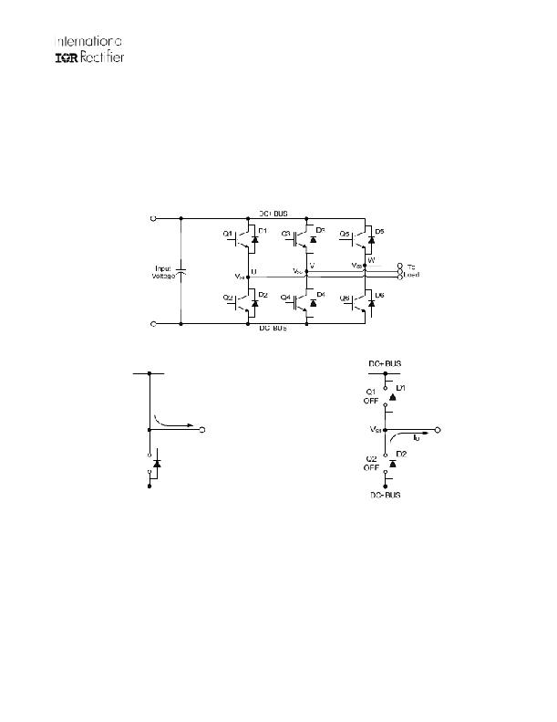
A common problem in today’s high-power switching converters is the transient response of the switch node’s
voltage as the power devices switch on and off quickly while carrying a large current. A typical 3-phase inverter
circuit is shown in Figure 11; where we define the power switches and diodes of the inverter.
If the high-side switch (e.g., the IGBT Q1 in Figures 12 and 13) switches off, while the U phase current is flowing
to an inductive load, a current commutation occurs from high-side switch (Q1) to the diode (D2) in parallel with the
low-side switch of the same inverter leg. At the same instance, the voltage node V S1 , swings from the positive DC
bus voltage to the negative DC bus voltage.
Figure 11: Three phase inverter
DC+ BUS
Q1
ON
I U
V S1
Q2
D2
OFF
DC- BUS
Figure 12: Q1 conducting
Figure 13: D2 conducting
Also when the V phase current flows from the inductive load back to the inverter (see Figures 14 and 15), and Q4
IGBT switches on, the current commutation occurs from D3 to Q4. At the same instance, the voltage node, V S2 ,
swings from the positive DC bus voltage to the negative DC bus voltage.
www.irf.com
17
? 2009 International Rectifier
发布紧急采购,3分钟左右您将得到回复。
相关PDF资料
IRS2607DSTRPBF
IC DVR MOSFET/IGBT N-CH 8-SOIC
IRS2608DSTRPBF
IC DRIVER MOSFET/IGBT 8-SOIC
IRS2609DSPBF
IC DVR MOSFET/IGBT N-CH 8-SOIC
IRS26302DJTRPBF
IC GATE DRIVER 3PH BRIDGE 44PLCC
IRS26310DJTRPBF
IC DRIVER MOSFET/IGBT 44-PLCC
IRS4427PBF
IC MOSFET DRIVER
IRS4427SPBF
IC DVR LOW SIDE DUAL 8-SOIC
IRS4428STRPBF
IC DVR LOW SIDE DUAL 8-SOIC
相关代理商/技术参数
IRS26072DSPBF_11
制造商:IRF 制造商全称:International Rectifier 功能描述:HIGH AND LOW SIDE DRIVER
IRS26072DSTRPBF
功能描述:功率驱动器IC Hlf-Brdg Drvr IC motion Cntrl IC
RoHS:否 制造商:Micrel 产品:MOSFET Gate Drivers 类型:Low Cost High or Low Side MOSFET Driver 上升时间: 下降时间: 电源电压-最大:30 V 电源电压-最小:2.75 V 电源电流: 最大功率耗散: 最大工作温度:+ 85 C 安装风格:SMD/SMT 封装 / 箱体:SOIC-8 封装:Tube
IRS2607DSPBF
功能描述:功率驱动器IC 600V High Low 10 to 20V 530ns RoHS:否 制造商:Micrel 产品:MOSFET Gate Drivers 类型:Low Cost High or Low Side MOSFET Driver 上升时间: 下降时间: 电源电压-最大:30 V 电源电压-最小:2.75 V 电源电流: 最大功率耗散: 最大工作温度:+ 85 C 安装风格:SMD/SMT 封装 / 箱体:SOIC-8 封装:Tube
IRS2607DSPBF
制造商:International Rectifier 功能描述:DRIVER
IRS2607DSTRPBF
功能描述:功率驱动器IC Half Bridge Drvr Hi Volt & Hi Speed
RoHS:否 制造商:Micrel 产品:MOSFET Gate Drivers 类型:Low Cost High or Low Side MOSFET Driver 上升时间: 下降时间: 电源电压-最大:30 V 电源电压-最小:2.75 V 电源电流: 最大功率耗散: 最大工作温度:+ 85 C 安装风格:SMD/SMT 封装 / 箱体:SOIC-8 封装:Tube
IRS2608DSPBF
功能描述:功率驱动器IC 600V Half-Bridge 10 to 20V 530ns RoHS:否 制造商:Micrel 产品:MOSFET Gate Drivers 类型:Low Cost High or Low Side MOSFET Driver 上升时间: 下降时间: 电源电压-最大:30 V 电源电压-最小:2.75 V 电源电流: 最大功率耗散: 最大工作温度:+ 85 C 安装风格:SMD/SMT 封装 / 箱体:SOIC-8 封装:Tube
IRS2608DSPBF_1
制造商:IRF 制造商全称:International Rectifier 功能描述:HALF-BRIDGE DRIVER
IRS2608DSTRPBF
功能描述:功率驱动器IC Hlf Brdg Drvr 600V .250A Compl Inpt
RoHS:否 制造商:Micrel 产品:MOSFET Gate Drivers 类型:Low Cost High or Low Side MOSFET Driver 上升时间: 下降时间: 电源电压-最大:30 V 电源电压-最小:2.75 V 电源电流: 最大功率耗散: 最大工作温度:+ 85 C 安装风格:SMD/SMT 封装 / 箱体:SOIC-8 封装:Tube
